
SMD CMOS Crystal Oscillator
Classification:
• Ultra Low Power Supply Voltage: 1.35-5.5V • Low Noise Typical: 0.3 pS at 12 kHz ~ 20 MHz Supply Options Frequency Offsets • Singled-end Output: CMOS • Temperature Range:-40~85°C Operation • Frequency Support from 1 MHz to 50MHz • Pb-free/RoHS Compliant
Email:
Wide temperature range
Ultra miniaturization
Ultra low jitter
High stability
Ultra-high frequency
Products
Product Details
FEATURES
• Ultra Low Power Supply Voltage: 1.35-5.5V
• Low Noise Typical: 0.3 pS at 12 kHz ~ 20 MHz Supply Options Frequency Offsets
• Singled-end Output: CMOS
• Temperature Range:-40~85°C Operation
• Frequency Support from 1 MHz to 50MHz
• Pb-free/RoHS Compliant
TYPICAL APPLICATION
• loT
• Game Console
• Smartphone
• Wearable Device
• Digital Camera
• Digital Consumer Electronics
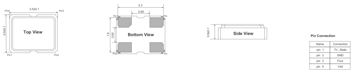
DIMENSIONS
ELECTRICAL SPECIFICATION
| Parameter | 3.3V | 2.5V | 1.8V | Unit | ||||
| min. | max. | min. | max. | min. | max. | |||
| Supply Voltage Variation(VDD) | VDD-5% | VDD+5% | VDD-5% | VDD+5% | VDD-5% | VDD+5% | V | |
| Frequency Range | 1 | 125 | 1 | 125 | 1 | 125 | MHz | |
| Supply Current | At 15pF Load | - | 25 | - | 25 | - | 20 | mA |
| No Load Condition,1MHz≤Fo<10MHz | - | 1.0 | - | 1.0 | - | 0.75 | mA | |
| No Load Condition,10MHz≤Fo<20MHz | - | 1.0 | - | 1.0 | - | 0.75 | mA | |
| No Load Condition,20MHz≤Fo<80MHz | - | 1.3 | - | 1.3 | - | 1.0 | mA | |
| No Load Condition,80MHz≤Fo<125MHz | - | 6 | - | 6 | - | 3 | mA | |
| Duty Cycle | 45 | 55 | 45 | 55 | 45 | 55 | % | |
| Output Level | Output High | 2.97 | - | 2.25 | - | 1.62 | - | V |
| Output Low | - | 0.33 | - | 0.25 | - | 0.18 | ||
|
Transition Time: Rise/Fall Time+ |
1.25MHz≤Fo<10MHz | - | 4 | - | 3 | - | 3 | nSec |
| 10MHz≤Fo<20MHz | - | 3 | - | 3 | - | 3 | nSec | |
| 20MHz≤Fo<80MHz | - | 2 | - | 2 | - | 2 | nSec | |
| Start-up time | - | 4 | - | 4 | - | 4 | mSec | |
| Tri-State (connect or Pin1) |
On (High Level or Floating) | 0.7VDD | - | 0.7VDD | - | 0.7VDD | - | V |
| Off(Low Level or Ground) | - | 0.3VDD | - | 0.3VDD | - | 0.3VDD | ||
| Output Load | 15 | 15 | 15 | pF | ||||
| Standby Current | - | 100 | - | 100 | - | 100 | uA | |
| Aging (@25°C,1st Year) | - | ±3 | - | ±3 | - | ±3 | ppm | |
| Storage Temp. Range | -55 | 125 | -55 | 125 | -55 | 125 | ℃ | |
| Phase Noise(Typ.) | TyP. | Max. | TyP. | Max. | TyP. | Max. | ||
|
At VDD=1.2V Fout=24MHz |
1 kHz offset | -130 | - | -133 | - | -135 | - | dBc/Hz |
| 10 kHz offset | -140 | - | -143 | - | -143 | - | ||
| 100 kHz offset | -148 | - | -150 | - | -150 | - | ||
| 1 MHz offset | -152 | - | -155 | - | -155 | - | ||
| Period Jitter(Pk-Pk) | - | 40 | - | 40 | - | 40 | pSec | |
| RMS Phase Jitter(Intergrated 12KHz~ 20MHz) | - | 1 | - | 1 | - | 1 | pSec | |
Standard frequencies are frequencies which the crystal has been designed and does not imply a stock position.
+ Transition times are measured between 20% and 80% of VDD.
FREO.STABILITY vs.TEMP. RANGE
| Temp.(℃) / ppm | ±20 | ±25 |
| -10~+60 | ⚪ | ⚪ |
| -20~+70 | ⚪ | ⚪ |
| -40~+85 | ▲ | ⚪ |
⚪:Available ▲:Condition ❌:Not available
*Inclusive of calilbration @ 25 °c, operating temperature range,input voltage variation,load variation, aging(1st year), shock, and vibration.
Note: not all combination of options are available, Other specifications may be available upon request.
Specifications subiect to change without notice.
Related Products
Message consultation
Free Product Manual, Leave Your Contact Information To Get It
Welcome Message
Leave Your Contact Information To Get A Free Product Quote
