Features of TC25A040000GECN11G
1. Standard 40 MHz High-Frequency Reference
40 MHz is one of the most widely used high-frequency clock references in digital systems, processor buses, and communication interfaces, with broad compatibility.
2. Ultra-High Frequency Stability (±0.5 ppm vs. Temperature)
Built-in temperature compensation circuit minimizes frequency drift caused by temperature changes, far superior to standard crystal oscillators, achieving high-precision frequency reference without external compensation.
3. High Frequency Tolerance (±1.5 ppm)
Exceptional initial accuracy, meeting the stringent frequency requirements of communication, navigation, and other critical systems.
4. Ultra-Wide Industrial Temperature Range (-40~85℃)
Covers the full industrial temperature range, suitable for harsh environments such as automotive electronics and industrial control.
5. Ultra-Low Power Consumption (2.0 mA)
Extremely low power for a TCXO, ideal for battery-powered portable devices and IoT terminals to extend battery life.
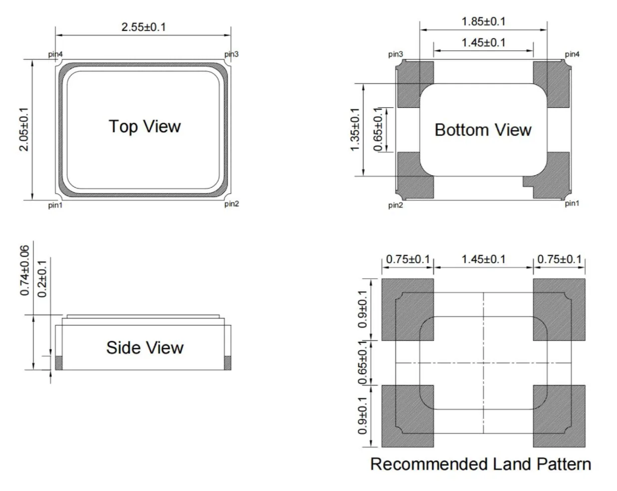
6. Miniature 2520 Package (2.5×2.0mm)
Compact form factor, suitable for space-constrained PCB layouts, supporting JEDEC standard reflow soldering.
7. Industry Applications
With its 40 MHz high-frequency output, ±0.5 ppm ultra-high temperature stability, ±1.5 ppm high tolerance, -40~85℃ industrial wide temperature range, 2.0 mA ultra-low power consumption, and 2520 miniature package, the TC25A040000GECN11G is widely used in 5G communication base stations, GPS/Beidou high-precision navigation, automotive electronics, industrial IoT terminals, test & measurement equipment, aerospace & defense, and medical devices that demand stringent high-frequency accuracy and temperature compensation.