Features of XO25D025000CCHE11G
1. Standard 25 MHz High-Frequency Reference
25 MHz is one of the most widely used high-frequency clock references in digital systems, processor buses, and communication interfaces, with extremely broad compatibility.
2. High Frequency Stability (±25 ppm)
Overall frequency stability of ±25 ppm meets the accuracy requirements of most communication, timing, and industrial control devices.
3. Wide Supply Voltage Range (1.60~3.63 V)
Supports a wide input voltage from 1.6 V to 3.63 V, compatible with mainstream system supply voltages such as 1.8 V and 3.3 V, offering flexible application.
4. Low Power Consumption (Only 15 mA)
Maintains low power consumption even at 25 MHz high-frequency output, ideal for battery-powered and portable devices.
5. Wide Operating Temperature Range (-20~70℃)
Covers the industrial temperature range, suitable for environments such as automotive electronics and industrial control.
6. Low Annual Aging (±3 ppm/year)
Outstanding long-term frequency stability, reducing the need for periodic calibration and lowering system maintenance costs.
7. Fast Start-up Time (5 ms)
Reaches stable output within 5 ms after power-on, meeting fast system start-up requirements.
8. Industry Applications
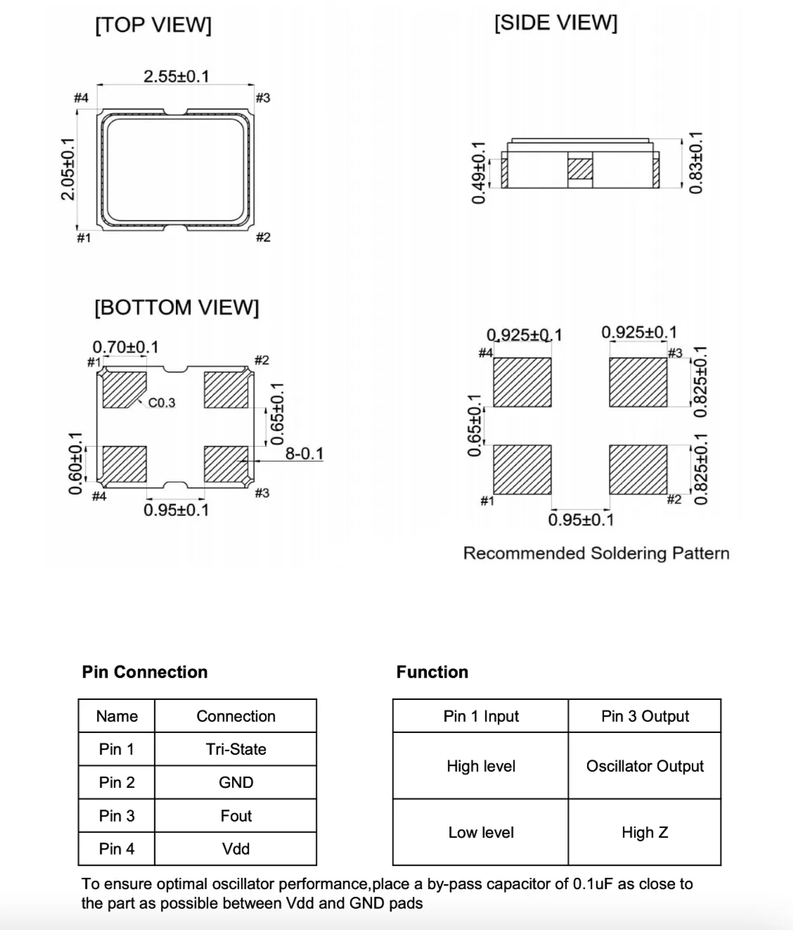
With its 25 MHz standard high-frequency clock, ±25 ppm high accuracy, wide supply voltage (1.6~3.63 V), low power consumption (15 mA), -20~70℃ wide operating temperature range, miniature 2520 package, and 10 rigorous reliability tests, the XO25D025000CCHE11G is widely used in consumer electronics, communication equipment, automotive electronics, industrial control, IoT terminals, smart meters, and medical devices that require high-frequency stable clock references.