Features of XO25F312500HDLE31A
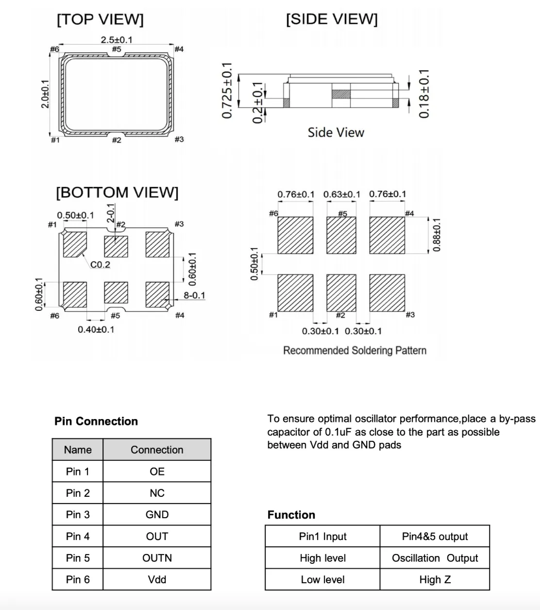
1. Ultra-Compact SMD 2520 Package
Description: Approx. 2.5×2.0×0.725 mm, suitable for high-density PCB layout and automated placement.
2. 312.500000 MHz High-Frequency Output
Description: Nominal frequency 312.500000 MHz, suitable for high-speed communications, optical modules, data centers, and other high-frequency clock applications.
3. LVDS Differential Output
Description: LVDS differential output with 100Ω load, providing strong anti-interference capability for high-speed differential clock transmission.
4. 3.3V Nominal Supply
Description: Supply voltage range 3.135–3.465 V, typical 3.300 V, suitable for standard 3.3V logic systems.
5. Wide Operating Temperature and High Frequency Stability
Description: Operating temperature -40 to +105°C, overall frequency stability ±20 ppm, suitable for stable clock output in harsh environments.
6. Ultra-Low Phase Jitter
Description: Phase jitter 30 fs-rms typ., 50 fs-rms max. over 12 kHz–20 MHz, helping reduce bit-error risk in high-speed SerDes, FPGA, and communication systems.
7. Low Power Consumption and Standby Function
Description: Operating current 38 mA max., standby current 60 µA max.; Pin 1 supports OE enable control, high level for output and low level for high impedance.
8. High-Speed Waveform Performance and High Reliability
Description: Rise/fall time 0.35 ns, duty cycle 45–55%, start-up time 10 ms max.; passes temperature cycling, aging, damp heat, UHAST, vibration, shock, and other reliability tests; compliant with Pb-free, RoHS 2.0, REACH, and HF.
9. Industry Applications
Description: Suitable for optical communications, data centers, network switching/routing, base stations, FPGA/SerDes, high-speed Ethernet, OTN, test and measurement, and other fields requiring a 312.5 MHz low-jitter LVDS clock; without confirmation, it must not be used in critical safety areas such as space technology, vehicle control, or military weapon development.