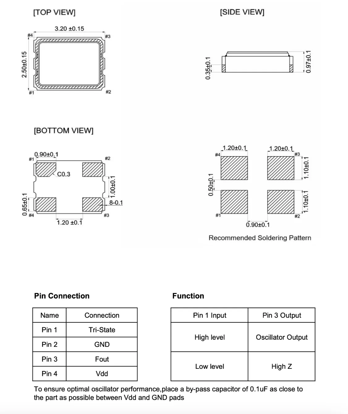
Features of XO32D024000GAHE11G
1. Compact SMD 3225 Package
Approx. 3.20×2.50×0.97 mm, suitable for high-density PCBs and automated placement.
2. Wide Supply Voltage Range
Supports 1.60–3.63 V, typical 2.80 V, compatible with 1.8 V, 2.5 V, and 3.3 V low-voltage systems.
3. Wide Operating Temperature and Overall Frequency Stability
Operating temperature -40 to +85°C, overall frequency stability ±50 ppm, including 25°C tolerance, temperature, voltage, load, and first-year aging.
4. CMOS Output and Load Capability
CMOS output, 15 pF load, duty cycle 45–55%, rise/fall time 8 ns max, VOH ≥ Vdd-0.4 V, VOL ≤ 0.4 V.
5. Tri-State Enable Control
Pin 1 supports tri-state control; high level enables oscillator output, low level gives high impedance, convenient for clock switching, testing, or power saving.
6. Low Current Consumption and Fast Start-Up
Description: Maximum operating current 15 mA, maximum start-up time 5 ms, suitable for systems requiring fast power-on clocking.
7. Low Aging and High Reliability
First-year aging ±3 ppm; passes low-temperature, damp heat, thermal shock, high-temperature operating life, vibration, mechanical shock, drop, solderability, and related reliability tests.
8. Environmental Compliance and Production Packaging
Pb-free, RoHS 2.0, REACH, HF; tape and reel 3000 pcs/reel; recommended reflow profile complies with JEDEC J-STD-020D.
9. Industry Applications
Suitable for general and specific electronic applications requiring a 24.000000 MHz CMOS clock, such as consumer electronics, industrial control, communication/networking, computers/peripherals, and portable devices; it must not be used in critical safety areas such as space technology, vehicle control, or military weapon development without confirmation.