Features of XO32F008000GAHE11G
1. Compact SMD 3225 Package
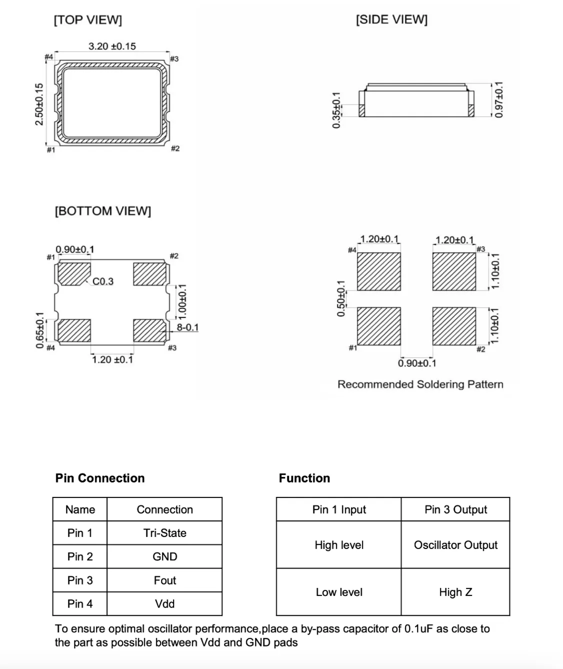
Approx. 3.20×2.50×0.97 mm, suitable for high-density PCB layout and automated placement.
2. 8.000000 MHz Nominal Frequency
Provides an 8.000000 MHz CMOS clock output, suitable for common clock scenarios such as MCU, communications, and consumer electronics.
3. 3.3V Nominal Supply with Wide Voltage Range
Supply voltage min. 2.97 V, typ. 3.30 V, max. 3.63 V, suitable for 3.3V logic systems.
4. CMOS Output and 15 pF Load Capability
CMOS output, 15 pF load, duty cycle 45–55%, rise/fall time 8 ns max, VOH ≥ Vdd-0.4 V, VOL ≤ 0.4 V.
5. Tri-State Enable Control
Pin 1 supports tri-state control; high level enables oscillator output, low level gives high impedance, convenient for clock switching, testing, or power saving.
6. Good Overall Frequency Stability and Aging
Overall frequency stability ±50 ppm, including 25°C tolerance, temperature, voltage, load, and first-year aging; first-year aging ±3 ppm.
7. Wide Operating Temperature, Low Power, and Fast Start-Up
Operating temperature -40 to +85°C, operating current 15 mA max, start-up time 5 ms max, suitable for systems requiring fast power-on clocking.
8. Environmental Compliance, Reliability, and Production Packaging
Pb-free, RoHS 2.0, REACH, HF; tape and reel 3000 pcs/reel; recommended reflow profile complies with JEDEC J-STD-020D, with multiple reliability tests passed.
9. Industry Applications
Suitable for general and specific electronic applications requiring an 8.000000 MHz CMOS clock, such as consumer electronics, industrial control, communication equipment, computer peripherals, and MCU systems; without confirmation, it must not be used in critical safety areas such as space technology, vehicle control, or military weapon development.