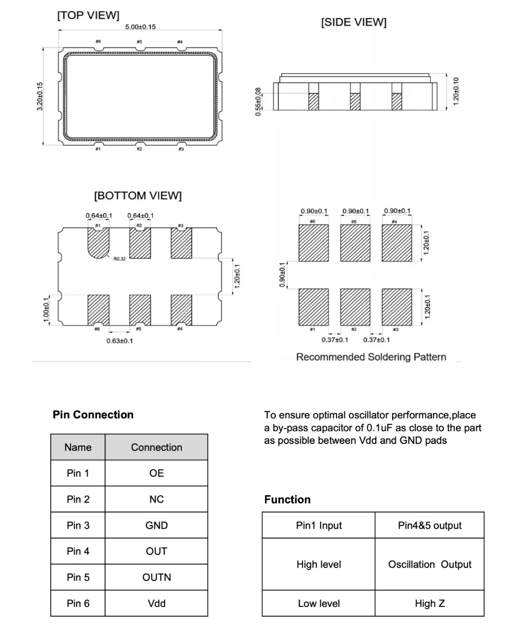
Features of XO50F200000GBLE11G
1. 200 MHz Ultra-High Frequency Reference
200 MHz is one of the most widely used high-frequency clock references in high-speed digital systems, communication base stations, and data centers, with broad compatibility and direct drive capability for FPGAs/ASICs.
2. LVDS Differential Output (OUT/OUTN)
Low-voltage differential signaling provides lent common-mode noise immunity and signal integrity, ideal for high-speed, long-distance transmission applications.
3. Ultra-Low Jitter (50 fs-rms, 12kHz~20MHz)
Extremely low phase noise and jitter ensure high-purity clock signals, meeting the stringent jitter requirements of 5G base stations and high-speed serial links.
4. Ultra-Fast Edge Rate (Rise/Fall Time 0.3 ns)
Extremely fast edge switching ensures steep signal edges, effectively minimizing timing jitter and signal distortion, ideal for ultra-high-speed digital systems.
5. Wide Operating Temperature Range (-40~85℃)
Covers the full industrial temperature range, suitable for harsh environments such as automotive electronics, industrial control, and outdoor communication equipment.
6. Low Annual Aging (±3 ppm/year)
Outstanding long-term frequency stability, reducing the need for periodic calibration and lowering system maintenance costs.
7. Industry Applications
With its 200 MHz ultra-high frequency clock, LVDS differential output with ultra-low jitter (50 fs-rms), ultra-fast edge rate (0.3 ns), ±30 ppm frequency stability, -40~85℃ wide operating temperature range, low-power standby, and 15 rigorous reliability tests, the XO50F200000GBLE11G is widely used in 5G communication base stations, high-speed data center interfaces, automotive electronics, industrial control, IoT gateways, smart meters, and medical devices that require high-frequency, low-jitter differential clock references.